


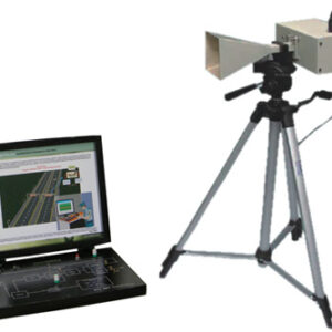
VLSI Design Trainer
This trainer has been designed with a view to provide practical and experimental Knowledge of VLSI Design technique on a P.C.B.
Description
This trainer has been designed with a view to provide practical and experimental Knowledge of VLSI Design technique on a P.C.B.
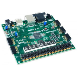
Programmable Logic Devices are playing major role in System Design due to their flexible architecture, re-programmability and fast time to market resulting in a smaller design-cycle period. Also lower design risk is involved with the use of PLDs because small design changes can be made without any PCB changes. The sigma’s
CPLD/FPGA boards have been designed to offer an platform for, low-cost system for designers / Students who need a flexible platform to gain exposure to the CPLD / FPGA device, or for those who need to rapidly prototype designs. These boards come with a power supply and programming cable, so designs can be implemented immediately without the need for any additional hardware. The experimental board includes almost all elements generally used in digital logic circuits, thus providing a complete training or a fast prototyping circuit design environment
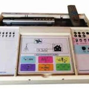
UNIVERSAL TRAINING KIT
This Universal PLD kit is an ideal trainer to implement and test the designs both for the beginner and the expert. It is “assembled ready” for various interfaces that include ADC/DAC, display, keyboard, RAM, serial communication etc. The user has to implement the design into the PLD using the given ucf. The Universal kit consists of a common mother board and various daughter boards. As the name says this is
a Universal Kit i.e. it has almost all the primary interfaces that a PLD may be used for. This Kit is designed to interface PLDs of any make (Xilinx, Altera, Actel etc…), any gate count and any package.
Features :
1. can use PLD (CPLD / FPGA) from any vendor
2. Any PLD / Package can be interfaced with it by designing new daughter board
3. The Daughter boards can be used as proto-boards input/output pins are brought out on four FRC connectors
4. 16 DIP Switch Inputs & 16 LED Outputs
5. 3×4 Keyboard Interface
6. 2 Key Inputs [Pulse]
7. Multiplexed 8 Digit / Non Multiplexed
8. 2 Digit 7 Segment display. (Selectable through jumper cable)
9. 8 Bit ADC Interface (ADC0804)
10. 8 Bit DAC Interface (TLC7528)
11. 64 K byte Memory Interface
12. I2C Interface
Reviews
There are no reviews yet.